My favourite retro-computing devices are those that are portable. The TRS-80 model 100 is especially interesting to me; it is a tablet computer released in 1983. I few days ago, I decided I should design my own portable computer.
Anyone who knows me in person knows that I am an avid supporter of the Motorola 68000, and other 68000-based CPUs. In my opinion, they are a much better design than the x86 architecture we are stuck with. For this reason, I decided to base my tablet around this CPU. Even though it was released in 1979, it is a very capable computing device. A 23 bit address bus and 16 bit data bus provides access to up to 16MB of address space, without having to use memory banking. Internally, the CPU is fitted with a large array of 32 bit general-purpose registers - 8 of them! That doesn't even include the 7 address registers and stack pointer register. Amazingly, this 40 year old CPU is still in production and used regularly; that's how good it is.
After picking the CPU, I added on pretty much whatever hardware I could think of. It has 1MB of ROM, up to 2MB of RAM, and 64K of EEPROM. On top of this, it features a CF card slot for mass storage, a mechanical keyboard, 2 serial ports, and a 240x64 screen. Physically, this takes up nearly all of the available board space.
The memory map is as follows:
| Address | Device | Size |
|---|---|---|
| 0xF10000 | I/O | 1MB - 64kB |
| 0xF00000 | EEPROM | 64kB |
| 0x20000 | RAM2 (optional) | 1MB |
| 0x10000 | RAM1 | 1MB |
| 0x0000 | ROM | 1MB |
Most of the address space is unused.
I will now walk-through some of the design I came up with. It was created in Kicad, which I have switched over to from Eagle.
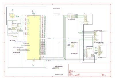
This is the general overview of the board. It only contains the CPU, the M68000, as well as the other pages that make up the computer. Other devices are not allowed to become bus masters, so the respective pins on the CPU are either left disconnected, or negated. Similarly, there is no circuitry to detect bus errors, so that pin is also negated.
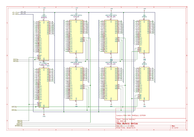
This is another fairly simple schematic. It contains the ROM, RAM, and EEPROM. Another page generates the chip select, lower read, and lower write signals used here. These are connected to each chip so that they talk to the address and data bus only when required.
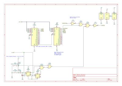
This page makes up the address decoder. It consists of two multiplexers, connected together. The first reads the upper 4 bits of the address bus, to determine which MB is selected. This is used to generate the ROM and RAM chip select signals. If the top MB of address space is selected, it enabled the second multiplexer. This multiplexer divides up the address space into 64kB chunks. The bottom chunk is reserved for the EEPROM. Each I/O device gets its own 64kB as well. It's overkill, but since the majority of the address space is unused, we don't give anything up by being inefficient.
This page is also responsible for generating the DTACK (data acknowledge) signal, which is asserted when the bus slave is done servicing its request. Only the serial controller uses this signal. All other devices are fast enough that we don't really need to worry about it. We can also abuse the DTACK line to allow single stepping. By negating the DTACK line by default, the CPU grinds to a halt. We can then apply a short pulse to the DTACK line whenever we want to step forward. The circuitry in the bottom left is responsible for generating a short pulse when the single step button is clicked.
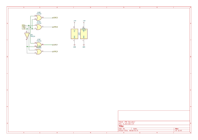
Another simple page. This takes the LDS (lower data select), UDS (upper data select), and R/W (read/write) signals from the CPU, and combines them in a way that makes sense to the memory chips.
As you can see, the data bus is connected directly to the CF card slot. The comment above it is out of date - it has a 16 bit connection to the bus. Enabling/disabling the slot is done by pulling the CS0 and CS1 lines high. However, the CPU still needs to be able to control them. This is done with the two OR gates, which allows a3 and a4 to pass through to CS0/CS1 when the card is enabled.
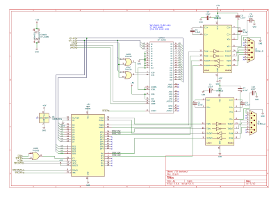
A 68681 is used as a serial port controller. It is able to support both ports. Two MAX232 ICs are used to boost the voltage to 12V for the RS-232 ports.
There are more pages, but I don't want to explain them all here as there are a lot of them. I have covered the most important ones.
For debugging, I have placed LEDs on the board that display the current address and data bus values. I will be writing a custom BIOS and OS from scratch to run on the device.
The full project is on my git server.
There is also a PDF of the schematics in "main/rev0".

